Views: 214 Author: Site Editor Publish Time: 2025-07-18 Origin: Site
Wafer dicing is one of the most critical processes in semiconductor manufacturing. It involves the precision separation of semiconductor wafers into individual dies using a wafer dicing machine. While this operation is essential for the functionality and packaging of integrated circuits (ICs), it is also fraught with various defects that can impact yield, performance, and reliability. In this article, we will explore the most common defects that arise during wafer dicing, their causes, and possible methods to mitigate them.
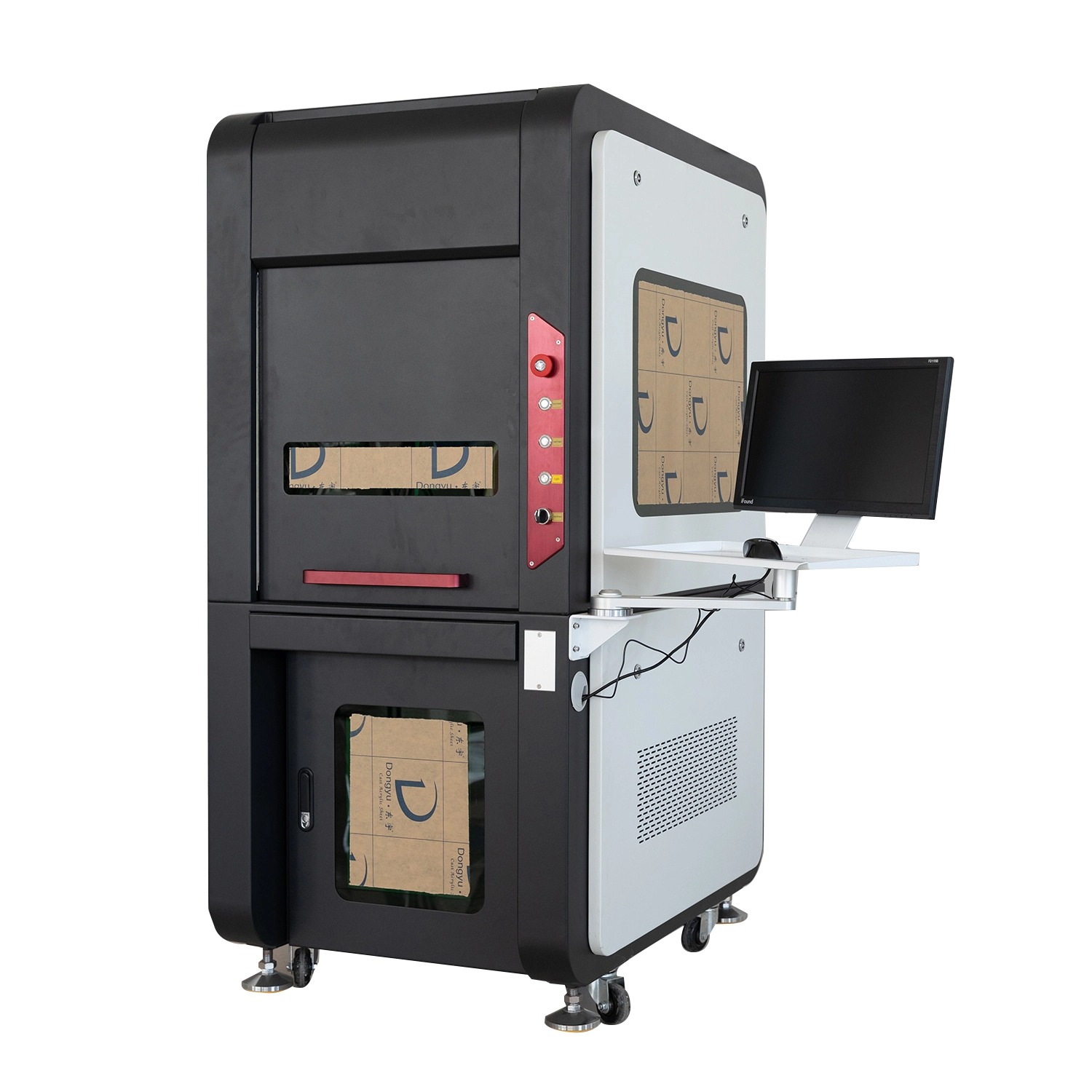
Wafer dicing is typically performed after wafer probing and before die bonding. The process involves cutting the wafer along scribe lines using methods such as blade dicing, laser dicing, or plasma dicing. The wafer dicing machine plays a central role in ensuring precision, cleanliness, and speed during this operation. However, due to the delicate nature of the materials involved—like silicon, gallium arsenide, or compound semiconductors—even small deviations in machine parameters or material inconsistencies can cause defects.
Let's delve into the most prominent types of wafer dicing defects that manufacturers frequently encounter.
Chipping is one of the most prevalent defects in wafer dicing. It refers to the micro-fractures or small pieces of silicon or other materials breaking away from the die during the cutting process. This typically occurs along the edge of the die, especially when using mechanical dicing blades.
Blade wear and degradation: As the dicing blade deteriorates over time, it loses sharpness, which increases lateral force on the wafer.
Improper spindle speed or feed rate: Incorrect machine parameters can introduce vibration or stress.
Material properties: Brittle materials like silicon carbide are more prone to edge chipping.
Chipping can reduce the reliability of ICs by exposing them to environmental contamination or electrical failure. In extreme cases, it can lead to outright die rejection. Proper maintenance of the wafer dicing machine and optimal blade selection are essential for controlling this defect.

Cracks—especially microcracks—are another serious concern. While larger cracks are visible to the naked eye or under a microscope, microcracks are often invisible but equally damaging. These defects can propagate over time, leading to die failure during packaging or in-field usage.
Excessive mechanical stress during the dicing process.
Inadequate chucking pressure, leading to vibration or die movement.
Thermal stress when using high-energy laser dicing without appropriate cooling.
Microcracks are often detected using non-destructive testing methods such as infrared inspection or scanning acoustic microscopy. To minimize their occurrence, manufacturers must fine-tune the process parameters of the wafer dicing machine and opt for techniques like stealth dicing, especially for ultra-thin wafers.
Burrs are tiny, often microscopic fragments of material that remain attached to the wafer after dicing. These can interfere with the pick-and-place process, cause die misalignment, or even short circuits if not removed properly.
Worn blades that don't cleanly cut the material.
High feed rates resulting in incomplete material separation.
Incorrect blade exposure or alignment.
Using finer grit blades, slowing the cutting speed, or incorporating cleaning systems within the wafer dicing machine can greatly reduce burr formation. Additionally, post-dicing plasma cleaning is often used to remove residual burrs.
Particle contamination doesn't always originate from the dicing blade itself. During the dicing process, tiny particles of silicon, adhesive tape residue, or coolant can settle on the wafer surface. These particles can interfere with bonding, degrade electrical performance, or trigger electrostatic discharge (ESD) failures.
Recirculated dicing coolant without proper filtration.
Operator handling or exposure to unclean environments.
Inadequate vacuuming or cleaning functions in the wafer dicing machine.
Upgrading filtration systems, using DI (deionized) water for rinsing, and operating in a cleanroom environment help mitigate particle-related defects. High-end wafer dicing machines also integrate advanced washing and drying modules to control contamination.
During dicing, wafers are mounted on dicing tape to hold them in place. However, improper adhesion or excessive blade force can cause the tape to peel or delaminate, leading to misaligned cuts or wafer breakage.
Low adhesion between tape and wafer due to poor-quality tape or surface contamination.
Excessive cutting depth causing blade contact with the tape.
Improper tape tensioning or wafer placement.
Select high-performance dicing tapes with consistent tackiness and elasticity. Calibrate the wafer dicing machine to maintain precise Z-height control, ensuring that blades don't dig into the tape.

When the adhesive bond weakens, or cutting vibrations are too strong, dies may become dislodged during or after the dicing process. This leads to die loss or damage, significantly reducing the yield.
Inadequate tape adhesion or degraded adhesive strength during extended dicing operations.
Excessive spindle vibration or machine misalignment.
Incorrect vacuum control during die separation.
Maintaining proper adhesive integrity, monitoring blade condition, and adjusting the wafer dicing machine's vacuum suction system can minimize this defect.
Here's a summary of the most common defects, their causes, and mitigation strategies:
| Defect | Primary Cause | Mitigation Strategy |
|---|---|---|
| Chipping | Blade wear, high feed rate | Use high-quality blades, reduce cutting speed |
| Microcracks | Thermal/mechanical stress | Optimize laser power, reduce mechanical force |
| Burr Formation | Worn blade, improper speed | Fine-grit blades, clean cut parameters |
| Particle Contamination | Coolant residue, ambient environment | DI water, HEPA filters, cleanroom conditions |
| Tape Delamination | Low-quality tape, excessive Z-depth | Better tape selection, precise machine calibration |
| Die Fly-off | Adhesive failure, vibration | Maintain vacuum, reduce mechanical shock |
Optimize all variables: choose the right blade, keep your wafer dicing machine well-maintained, calibrate feed rates, and conduct post-dicing inspections. A holistic approach will yield better results.
Cooling—usually with DI water or air—is critical to prevent thermal cracks and reduce debris accumulation. Cooling also extends the life of the dicing blade.
Not necessarily. While laser dicing can introduce thermal stress, it also reduces mechanical chipping. Proper parameter control can make laser dicing very reliable.
It depends on the material and volume. Monitor for signs of increased chipping or burrs—these often signal blade degradation.
The wafer dicing process, though seemingly straightforward, requires meticulous attention to detail and an understanding of the physics behind each defect. Each imperfection—from chipping to particle contamination—can be traced back to controllable process variables within the wafer dicing machine or the operating environment.
To minimize defects, manufacturers must invest in proper equipment maintenance, high-quality consumables, and optimized process control. Doing so not only improves yield but also enhances device performance, durability, and overall manufacturing efficiency. Ultimately, mastering wafer dicing is not just about slicing silicon—it's about cutting through complexity with precision.